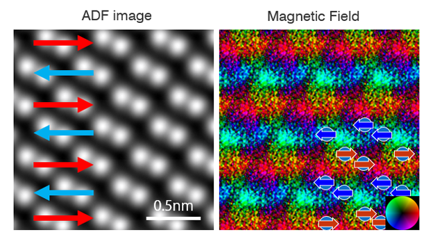
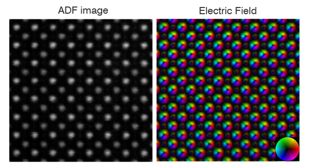
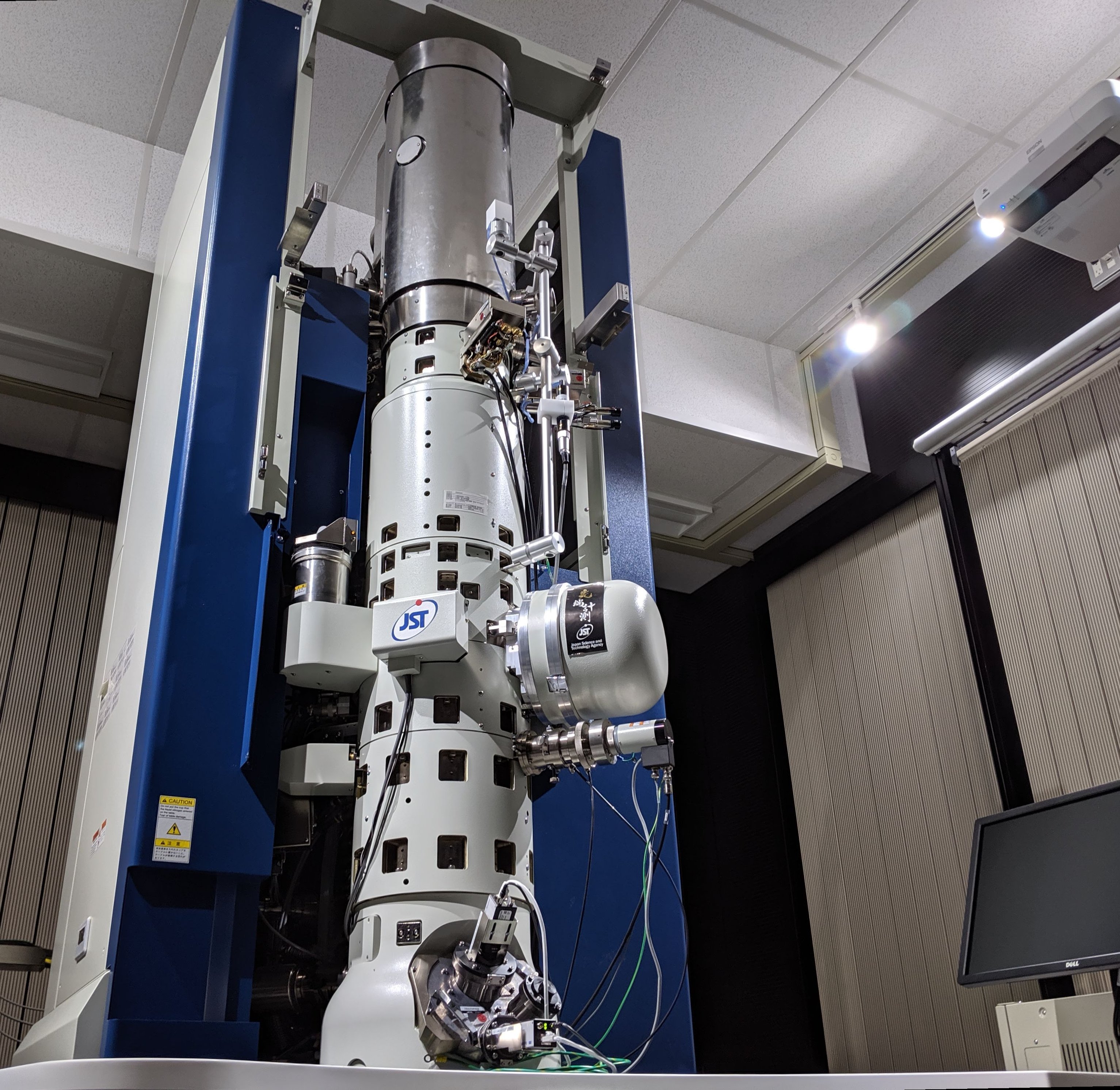
In this laboratory, we are conducting research aimed at elucidating the fundamental mechanisms of material interface properties from the atomic and electronic scales, with the development of the state-of-the-art atomic resolution electron microscopy. In particular, the evolution of electron microscopes in recent years is remarkable, and it is becoming possible to visualize the world below atomic size. We aim to clarify the fundamental principles of materials by further developing the state-of-the-art electron microscopy.

Official HP: https://www.saaf.t.u-tokyo.ac.jp/nshibata?lang=en

img-slide-electron-microscopy-and-materials-science-lab-04
img-slide-electron-microscopy-and-materials-science-lab-05
img-slide-electron-microscopy-and-materials-science-lab-02
img-slide-electron-microscopy-and-materials-science-lab-03

メンバー

  • 柴田直哉4-2

    Professor

    Naoya SHIBATA

    Electron Microscopy and Materials Science Laboratory

    Institute of Engineering Innovation, School of Engineering

  • profimg-advanced-nanocharacterization center-takehito-seki

    Assistant Professor

    Takehito SEKI

    Electron Microscopy and Materials Science Laboratory

    Electron microscopy, metallurgy

  • profimg_33_遠山慧子

    Assistant Professor

    Satoko TOYAMA

    Electron Microscopy and Materials Science Laboratory

  • 川原一晃kawahara

    Assistant Professor

    kazuaki KAWAHARA

    High Voltage Electron Microscope Laboratory

  • 近藤隼mkondo

    Assistant Proffessor

    Syun KONDO

    High Voltage Electron Microscope Laboratory

    High Voltage Electron Microscope Laboratory

  • profimg_29_佐々野駿

    Project Assistant Professor

    Shun SASANO

    Electron Microscopy and Materials Science Laboratory

  • 幾原雄一 Yuichi Ikuhara3

    特別研究教授

    Yuichi IKUHARA